
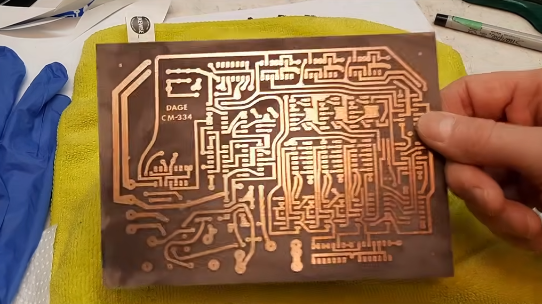
In the era before PCB shops would make almost any PCB imaginable, as well making many other manufacturing processes for prototypes available to hobbyists, there were several ways of making PCBs at home. Many of which involve harsh chemicals and were easy to mess up. Getting a single-layer PCB using the toner transfer method, for example, took a bit of practice (and a fume hood) to get right. [Bettina Neumryr] is working on a custom two-layer PCB, and has a new trick to get it to come out right despite the added complexity of the second layer.
The method starts out as a standard single-layer board in effect. Toner is ironed onto a copper board, in this case using a laminator, which allows the board to go into an acid bath which washes away all of the un-tonered copper. But with the second layer exposed, this would wash away the other side of the board completely. [Bettina] is using a new method here to protect that layer during the first bath: covering it in ink from a magic marker. With the first board etched, the ink and toner get washed off and the second layer is carefully lined up, put through the laminator, and then the opposite side gets covered in ink for the second acid bath.
After the process is complete and many layers of ink and toner are removed, [Bettina] is left with a PCB that’s ready to receive electronic components, if a little stained from all the ink. As to what this specific board is going to be used for, she’s kept that a bit cryptic as it’s the subject of a future video. Her builds usually revolve around designs from antique elecronics magazines, so it’s almost certainly something of that nature, and that’s also why this specific design couldn’t be just sent off to a board shop.